Product Summary
EP2AGX190FF35I3N absolute maximum ratings: (1)VCC Supplies power to the core, periphery, I/O registers, PCI Express (PIPE) (PCIe) HIP block, and transceiver PCS: -0.5 to 1.35 V; (2)VCCCB Supplies power for the configuration RAM bits: -0.5 to 1.8 V; (3)VCCBAT Battery back-up power supply for design security volatile key register: -0.5 to 3.75 V; (4)VCCPD Supplies power to the I/O pre-drivers, differential input buffers, and MSEL circuitry: -0.5 to 3.75 V; (5)VCCIO Supplies power to the I/O banks: -0.5 to 3.9 V; (6)VCCD_PLL Supplies power to the digital portions of the PLL: -0.5 to 1.35 V; (7)VCCA_PLL Supplies power to the analog portions of the PLL and device-wide power
Parametrics
EP2AGX190FF35I3N absolute maximum ratings: (1)VCC Supplies power to the core, periphery, I/O registers, PCI Express (PIPE) (PCIe) HIP block, and transceiver PCS: -0.5 to 1.35 V; (2)VCCCB Supplies power for the configuration RAM bits: -0.5 to 1.8 V; (3)VCCBAT Battery back-up power supply for design security volatile key register: -0.5 to 3.75 V; (4)VCCPD Supplies power to the I/O pre-drivers, differential input buffers, and MSEL circuitry: -0.5 to 3.75 V; (5)VCCIO Supplies power to the I/O banks: -0.5 to 3.9 V; (6)VCCD_PLL Supplies power to the digital portions of the PLL: -0.5 to 1.35 V; (7)VCCA_PLL Supplies power to the analog portions of the PLL and device-wide power management circuitry: -0.5 to 3.75 V; (8)VI DC input voltage: -0.5 to 4.0 V; (9)IOUT DC output current, per pin: -25 to 40 mA; (10)VCCA Supplies power to the transceiver PMA regulator: 3.75 V; (11)VCCL_GXB Supplies power to the transceiver PMA TX, PMA RX, and clocking: 1.21 V; (12)VCCH_GXB Supplies power to the transceiver PMA output (TX) buffer: 1.8 V; (13)TJ Operating junction temperature: -55℃ to 125℃; (14)TSTG Storage temperature (no bias): -65℃ to 150℃.
Features
EP2AGX190FF35I3N features: (1)40-nm, low-power FPGA engine; (2)High-performance digital signal processing (DSP) blocks up to 550 MHz; (3)Maximum system bandwidth; (4)Complete PIPE protocol solution with an embedded hard IP block; (5)Optimized for high-bandwidth system interfaces; (6)Low power; (7)Advanced usability and security features; (8)Emulated LVDS output support with a data rate of up to 1152 Mbps.
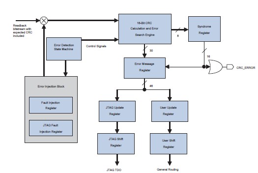
Diagrams

| Image | Part No | Mfg | Description |  |
Pricing (USD) |
Quantity | ||||||
|---|---|---|---|---|---|---|---|---|---|---|---|---|
 |
 EP2AGX190FF35I3N |
 |
 IC ARRIA II GX 190K 1152FBGA |
 Data Sheet |

|
|
||||||
| Image | Part No | Mfg | Description |  |
Pricing (USD) |
Quantity | ||||||
 |
 EP2A25F672C9 |
 Other |
 |
 Data Sheet |
 Negotiable |
|
||||||
 |
 EP2AGX125DF25C4 |
 |
 IC ARRIA II GX FPGA 125K 572FBGA |
 Data Sheet |

|
|
||||||
 |
 EP2AGX125DF25C4N |
 |
 IC ARRIA II GX FPGA 125K 572FBGA |
 Data Sheet |

|
|
||||||
 |
 EP2AGX125DF25C5 |
 |
 IC ARRIA II GX FPGA 125K 572FBGA |
 Data Sheet |

|
|
||||||
 |
 EP2AGX125DF25C5N |
 |
 IC ARRIA II GX FPGA 125K 572FBGA |
 Data Sheet |

|
|
||||||
 |
 EP2AGX125DF25C6 |
 |
 IC ARRIA II GX FPGA 125K 572FBGA |
 Data Sheet |

|
|
||||||
 (Hong Kong)


